LEAP OBT 12-TRX 192G NRZ - RUGGED
Contact:
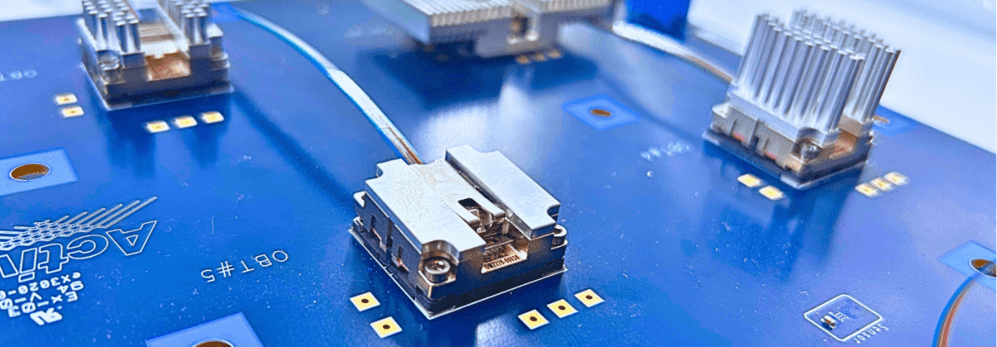
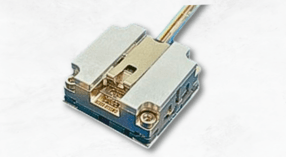
The LEAP® On-Board Transceiver is a rugged 12-channel duplex optical transceiver capable of running data-rates of up to 16Gbps per channel (192Gbps cumulative) on multi-mode fiber:
- Operating case temperature: (-40°C;+85°C)
- Shock: (500g;1ms) per MIL STD-883 Method 2002.4
- Vibration: 20g@[20-2000Hz] per MIL STD-883 Method 2007.3
The LEAP® On-Board Transceiver has first been introduced by AAOP in its commercial version (12TRx; 25Gbps per channel; 300Gbps aggregate in each direction) in 2015 to serve the needs for high-density and high-data rate applications in datacenters, supercomputers and 5G broadband infrastructures.
AAOP added the rugged version of its LEAP OBT to its portfolio in 2020.
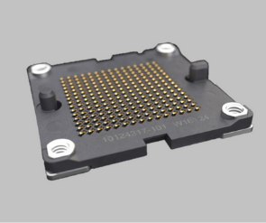
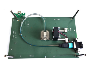
The LEAP OBT is connected to the PCB using a dedicated BGA socket and four screws. The optical interface fits a MT24 ferule which is fixed onto the module by means of a clip.
- Small footprint (1inchx1inch) allows for an optimal space-saving solution
- Data rate transparent from 300Mbps to 16 Gbps*
- Fiber connection via standard MT24 ferrule – Separable Interface
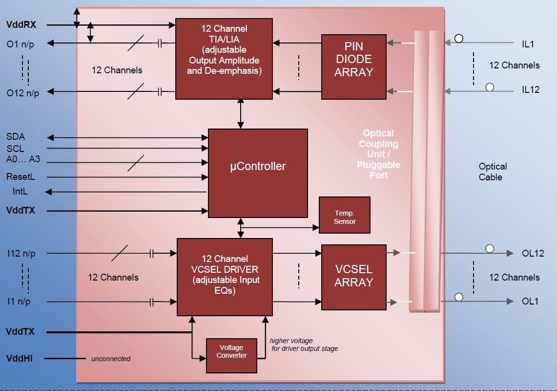
- Two-wire control and diagnostic interface (i²c)
- Temperature monitoring
- Input voltage (module)
- Rx Power monitoring (RSSI)
- Programmable input equalization
- Programmable output amplitude and de-emphasis
- Low power consumption (0.3W average per channel at 10Gbps Tx+Rx)
- High optical link-budget (14dB nominal at 10 Gbps, PRBS31)
*Amphenol can provide the fiber optic cables on request (e.g. MT-MPO or MT-fanouts)
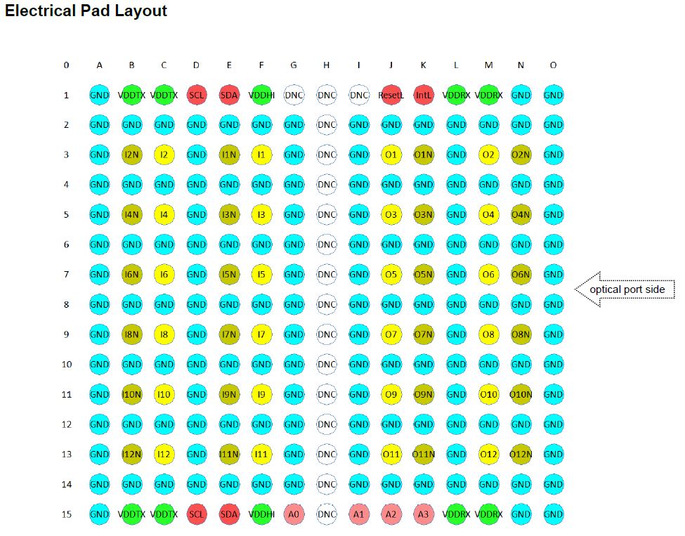
OBT Pad Layout (view through the transceiver on host board connector) / DNC = Do Not Connect
| PIN | Symbol | I/O | Description |
| F3,E3 | I1, I1N | Input | TxChannel 1, Differential Transmitter Data Input, AC coupled |
| C3,B3 | I2, I2N | Input | TxChannel 2, Differential Transmitter Data Input, AC coupled |
| F5,E5 | I3, I3N | Input | TxChannel 3, Differential Transmitter Data Input, AC coupled |
| C5,B5 | I4, I4N | Input | TxChannel 4, Differential Transmitter Data Input, AC coupled |
| F7,E7 | I5, I5N | Input | TxChannel 5, Differential Transmitter Data Input, AC coupled |
| C7,B7 | I6, I6N | Input | TxChannel 6, Differential Transmitter Data Input, AC coupled |
| F9,E9 | I7, I7N | Input | TxChannel 7, Differential Transmitter Data Input, AC coupled |
| C9,B9 | I8, I8N | Input | TxChannel 8, Differential Transmitter Data Input, AC coupled |
| F11,E11 | I9, I9N | Input | TxChannel 9, Differential Transmitter Data Input, AC coupled |
| C11,B11 | I10, I10N | Input | TxChannel 10, Differential Transmitter Data Input, AC coupled |
| F13,E13 | I11, I11N | Input | TxChannel 11, Differential Transmitter Data Input, AC coupled |
| C13,B13 | I12, I12N | Input | TxChannel 12, Differential Transmitter Data Input, AC coupled |
| A1 to A15 | GND | Power | Common Ground |
| B2,B4,B6,B8,B10,B12,B14 | GND | Power | Common Ground |
| C2,C4,C6,C8,C10,C12,C14 | GND | Power | Common Ground |
| D2 to D14 | GND | Power | Common Ground |
| E2,E4,E6,E8,E10,E12,E14 | GND | Power | Common Ground |
| F2,F4,F6,F8,F10,F12,F14 | GND | Power | Common Ground |
| G2 to G14 | GND | Power | Common Ground |
| G1, H1 to H14,I1 | DNC | (reserved) | |
| H15 | Do not connect these pins on host board, reserved for OBT module. | ||
| H15 is used by Amphenol for firmware programming. | |||
| I2 to I14 | GND | Power | Common Ground |
| J2,J4,J6,J8,J10,J12,J14 | GND | Power | Common Ground |
| K2,K4,K6,K8,K10,K12,K14 | GND | Power | Common Ground |
| L2 to L14 | GND | Power | Common Ground |
| M2,M4,M6,M8,M10,M12,M14 | GND | Power | Common Ground |
| N1,N2,N4,N6,N8,N10,N12,N14, N15 | GND | Power | Common Ground |
| O1 to O15 | GND | Power | Common Ground |
| B1,C1,B15,C15 | VDDTX | Power | Power Supply Transmit Side |
| F1,F15 | VDDHI | Power | not used, not connected inside OBT |
| L1,M1,L15,M15 | VDDRX | Power | Power Supply Receiver Side |
| D1,D15 | SCL | Input | I2C, Serial Clock, need Pull-up resistor on host board, SCL pins D1 and D15 are connected together inside OBT |
| E1,E15 | SDA | Input/Output | I2C, Serial Data, need Pull-up resistor on host board, SDA pins E1 and E15 are connected together inside OBT |
| G15 | A0 | Input | I2C Address Line, internal 10k Pull-up resistor to VDDTX |
| I15 | A1 | Input | I2C Address Line, internal 10k Pull-up resistor to VDDTX |
| J15 | A2 | Input | I2C Address Line, internal 10k Pull-up resistor to VDDTX |
| K15 | A3 | Input | I2C Address Line, internal 10k Pull-up resistor to VDDTX |
| J1 | ResetL | Input | Module Reset, internal 10k Pull-up resistor to VDDTX |
| K1 | IntL | Output | Interrupt Low, need Pull up resistor on host board |
| J3,K3 | O1, O1N | Output | RxChannel 1, Differential Receiver Data Output, AC coupled |
| M3,N3 | O2, O2N | Output | RxChannel 2, Differential Receiver Data Output, AC coupled |
| J5,K5 | O3, O3N | Output | RxChannel 3, Differential Receiver Data Output, AC coupled |
| M5,N5 | O4, O4N | Output | RxChannel 4, Differential Receiver Data Output, AC coupled |
| J7,K7 | O5, O5N | Output | RxChannel 5, Differential Receiver Data Output, AC coupled |
| M7,N7 | O6, O6N | Output | RxChannel 6, Differential Receiver Data Output, AC coupled |
| J9,K9 | O7, O7N | Output | RxChannel 7, Differential Receiver Data Output, AC coupled |
| M9,N9 | O8, O8N | Output | RxChannel 8, Differential Receiver Data Output, AC coupled |
| J11,K11 | O9, O9N | Output | RxChannel 9, Differential Receiver Data Output, AC coupled |
| M11,N11 | O10, O10N | Output | RxChannel 10, Differential Receiver Data Output, AC coupled |
| J13,K13 | O11, O11N | Output | RxChannel 11, Differential Receiver Data Output, AC coupled |
| M13,N13 | O12, O12N | Output | RxChannel 12, Differential Receiver Data Output, AC coupled |
